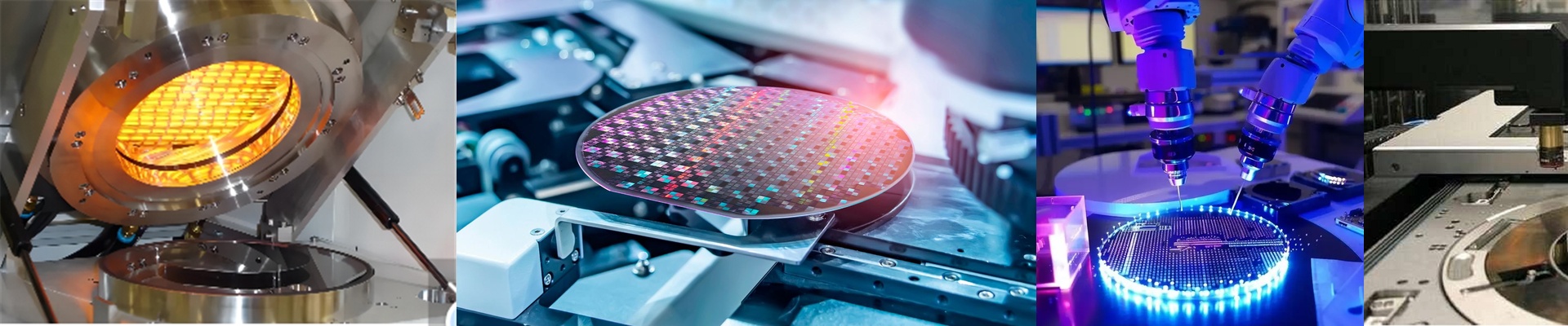
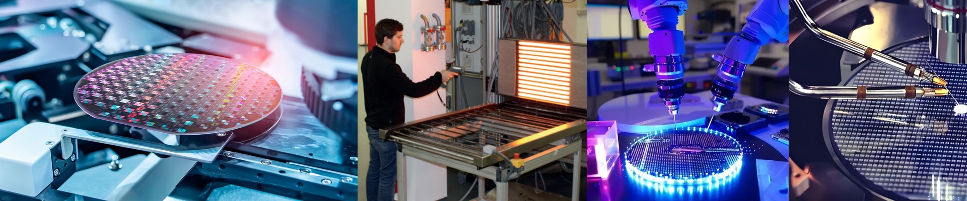

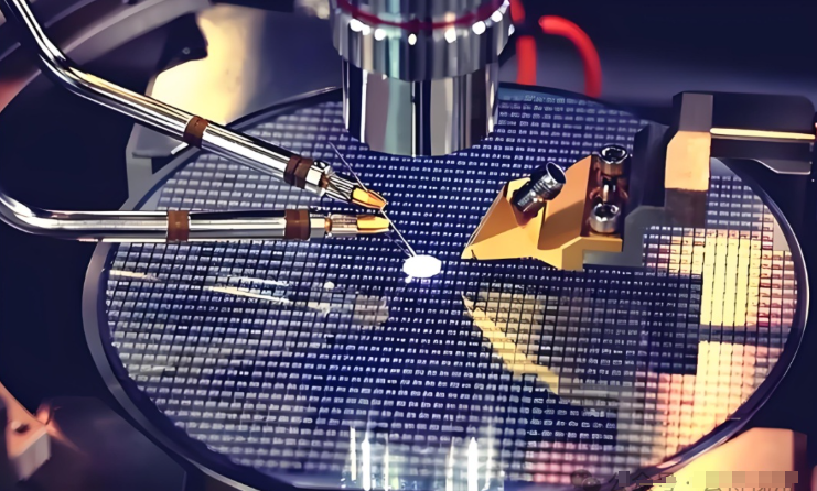
On the fab floor, Wafer thinning is a thermally sensitive operation. A non-uniform heat profile during infrared heating doesn’t just distort the wafer; it drives yield loss through warpage, photoresist stress, and micro-cracks that show up later in lithography and packaging. You need a heat source that treats the entire surface as one repeatable thermal zone. What Matters Technically Our short-wave infrared heating modules hold wafer-level uniformity within ±0.1°C across the entire substrate, with response times under 2 seconds and stable setpoints from room temperature to 450°C. The emitter array uses quartz-halogen elements in a reflector geometry that minimizes hot spots, and the thermal system is built for Class 1–100 cleanroom operation with zero particle generation during steady state. Temperature repeatability stays better than ±0.5°C over 5,000+ hours, which keeps soft bake and hard bake profiles consistent for the photoresist. Why It Works Here Wafer thinning needs heat without contamination and without thermal gradients that induce stress. The infrared energy punches through thin substrates quickly, cutting thermal budget and cycle time while keeping dimensional stability. The payoff is fewer scrapped wafers, stable critical dimension control, and predictable film adhesion after the bake. Energy use drops because the module heats on demand and cools fast, and the low-maintenance design keeps unplanned downtime off the schedule. Things to Know Installation comes down to precise optical alignment between the emitter array and the wafer plane, and the system needs clean, dry air to keep the quartz window free of condensation. The module is compatible with SECS/GEM for integration, but it won’t cover for poor wafer chucking; the chuck has to provide uniform backside contact to hit that full ±0.1°C uniformity. Plan the interface early, and the process window opens right away.